Model 845 Microwave Signal Generator (9 kHz to 26.5 GHz)
Versatile single-channel microwave and RF source covering 9 kHz to 26.5 GHz with ultra-low phase noise, fast switching, and broad VLF-through-K-band coverage.
Specifications reproduced from Model 845 datasheet V2.76 (dc-81405202). Warranted at 23 ±5 °C after 30-minute warm-up unless stated.
1Introduction
Very compact, portable analog signal generator models with a range from 9 kHz (with option 9K) up to 26.5 GHz. The Model 845 is a series of low-noise and fast-switching microwave signal generators covering continuous frequency ranges from as low as 100 kHz up to 12, 20, and 26 GHz, respectively, with a 0.001 Hz resolution.
The Model 845 provides an accurately leveled output power range and high spurious suppression. Advanced frequency synthesis with fractional-N divider makes for low SSB phase noise and micro-Hz resolution.
The standard Model 845 includes amplitude modulation (AM), DC-coupled low-distortion wideband frequency modulation (FM), PM, FSK and PSK, frequency chirp, and fast pulse modulation with internal pulse train generator. Three internal modulation sources are available. All modulation modes of the Model 845 can be combined. This allows the generation of complex modulation signals for modern communication and location systems. The combination of pulse modulation and FM simulates Doppler effects or chirp signals. Simultaneous AM and pulse modulation provide the types of signal occurring in pulse radar applications with rotating antenna. The combination of FM and AM can be used to check fading effects of FM receivers.
All Model 845 units allow fast analog and digital sweeps including flexible list sweeps, where frequency, power, and dwell times can be set individually. A flexible triggering capability simplifies synchronization within test environments.
All Model 845 units operate with an ultra-stable temperature-compensated 100 MHz reference (OCXO) to ensure minimal drift, and can be phase-locked to any stable external reference in a range from 1 to 250 MHz. Additionally, optimum phase-synchronous signals can be achieved by bypassing the internal reference and feeding a 100 MHz signal directly as reference. The 845 supports various standard interfaces such as USB-TMC, LAN, and GPIB.
Definitions
The specifications in the following pages describe the warranted performance of the instrument for 23 ±5 °C after a 30-minute warm-up period, unless otherwise stated.
Min/Max: Parameter range that is guaranteed by product design, and/or production tested. Warranted performance specifications include guard-bands to account for the expected statistical performance distribution, measurement uncertainties, and changes in performance due to environmental conditions.
Typical: Expected mean values, not warranted performance.
Applications
R&D low-noise microwave source
Production testing (industry-leading switching times, high dynamic range)
Service and maintenance (battery operation)
Signal simulation (Radar, WiMax, UWB)
Aerospace & defense (pulse modulator, chirps)
2Available Options
Option
Description
HP
Delivers higher maximum output power, to a level up to +27 dBm.
PE2
Optional power level extension to accurately level below -120 dBm.
FS
Substantially enhances the switching speed.
9K
Low-frequency extension down to 9 kHz (845-20, 845-12 only).
1URM
Modifies the form factor to a 19" rack-mountable 1HU enclosure.
FILT
Harmonic filtering.
3Frequency Parameters & Range
Parameter
Min
Typical
Max
Note
Frequency range
845-12
100 kHz
12.0 GHz
845-20
100 kHz
20.0 GHz
Settable to 20.5 GHz
845-26
100 kHz
26.0 GHz
Settable to 30 GHz
Option 9 kHz
9 kHz
Low-frequency extension
Resolution
0.001 Hz
Phase resolution
0.1 deg
Frequency / amplitude setting time
Standard
200 µs
300 µs
Option FS
30 µs
Option NEC
30 µs
Fstep < 2.2 GHz
4Level Performance
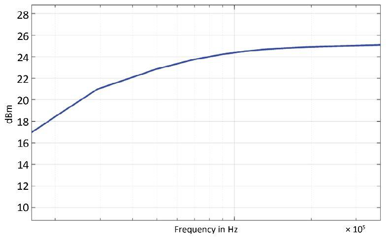
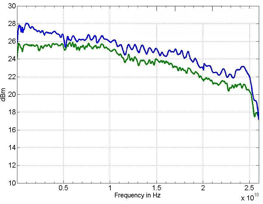
Output power. Check the maximum output power plots below. Level resolution is 0.01 dB.
Figure 1: Typical Maximum Output Power from 9 kHz to 1 MHz (option 9K).Figure 2: Maximum Output Power 845-26, HP with and without option PE2.
Configuration / frequency range
Min
Max
Standard
9 kHz to 100 kHz (option 9K)
-20 dBm
+15 dBm
100 kHz to 26 GHz
-20 dBm
+15 dBm
Option PE
9 kHz to 100 kHz (option 9K)
-90 dBm
+13 dBm
100 kHz to 26 GHz
-90 dBm
+13 dBm
Option PE2
9 kHz to 100 kHz (option 9K)
-120 dBm
+13 dBm
100 kHz to 26 GHz
-120 dBm
+13 dBm
Option HP
9 kHz to 100 kHz (option 9K)
-20 dBm
+15 dBm
100 kHz to 10 MHz
-20 dBm
+20 dBm
0.01 to 12 GHz
-20 dBm
+21 dBm
12 to 20 GHz
-20 dBm
+20 dBm
20 to 24 GHz
-20 dBm
+19 dBm
24 to 26 GHz
-20 dBm
+15 dBm
Option HP and FILT
9 kHz to 100 kHz (option 9K)
-20 dBm
+15 dBm
100 kHz to 10 MHz
-20 dBm
+19 dBm
0.01 to 12 GHz
-20 dBm
+20 dBm
12 to 20 GHz
-20 dBm
+19 dBm
20 to 24 GHz
-20 dBm
+18 dBm
24 to 26 GHz
-20 dBm
+14 dBm
Option HP and PE2
9 kHz to 100 kHz (option 9K)
-120 dBm
+13 dBm
100 kHz to 10 MHz
-120 dBm
+20 dBm
0.01 to 12 GHz
-120 dBm
+21 dBm
12 to 20 GHz
-120 dBm
+19 dBm
20 to 24 GHz
-120 dBm
+18 dBm
24 to 26 GHz
-120 dBm
+14 dBm
Options HP and PE2 + FILT
9 kHz to 100 kHz (option 9K)
-120 dBm
+13 dBm
100 kHz to 10 MHz
-120 dBm
+19 dBm
0.01 to 12 GHz
-120 dBm
+20 dBm
12 to 20 GHz
-120 dBm
+18 dBm
20 to 24 GHz
-120 dBm
+17 dBm
24 to 26 GHz
-120 dBm
+13 dBm
Options HP and PE
9 kHz to 100 kHz (option 9K)
-90 dBm
+13 dBm
100 kHz to 10 MHz
-90 dBm
+20 dBm
0.01 to 12 GHz
-90 dBm
+21 dBm
12 to 20 GHz
-90 dBm
+19 dBm
20 to 24 GHz
-90 dBm
+18 dBm
24 to 26 GHz
-90 dBm
+14 dBm
Option HP and PE + FILT
9 kHz to 100 kHz (option 9K)
-90 dBm
+13 dBm
100 kHz to 10 MHz
-90 dBm
+19 dBm
0.01 to 12 GHz
-90 dBm
+20 dBm
12 to 20 GHz
-90 dBm
+18 dBm
20 to 24 GHz
-90 dBm
+17 dBm
24 to 26 GHz
-90 dBm
+13 dBm
5Power Uncertainty & VSWR
Reverse Power Protection and VSWR
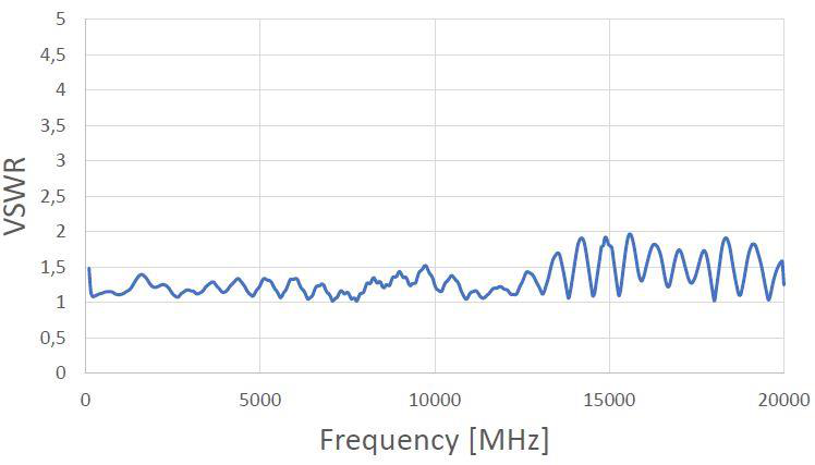
Figure 3: Typical VSWR (845-20).
Parameter
Min
Typical
Max
Note
Reverse power protection — DC voltage
±15 V
Reverse power protection — RF power
+30 dBm
Output impedance
50 Ω
VSWR
< 20 GHz
1.5
> 20 GHz
2.0
Power Level Uncertainty (ALC on, Model 845 + PE2/PE)
Values are the warranted figure, with the typical value in parentheses.
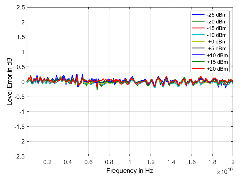
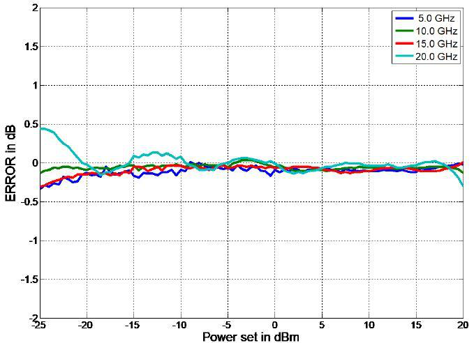
Figure 4: Typical Frequency Response 0 to 20 GHz at -20, 0, and +20 dBm (level error versus frequency).Figure 5: Typical Frequency Response 0 to 20 GHz at -20, 0, and +20 (level error versus power set).
Frequency
>15 dBm to Pmax
-15 to +15 dBm
-70 to -15 dBm
< -70 dBm
10 MHz to 10 GHz
1.6 dB (0.8 dB)
1.0 dB (0.3 dB)
1.5 dB (0.4 dB)
1.8 dB (0.5 dB)
100 Hz to fmax
1.6 dB (0.8 dB)
1.0 dB (0.3 dB)
1.5 dB (0.4 dB)
2.0 dB (0.5 dB)
User flatness correction: up to 2000 points. Temperature effects: 0.015 dB/°C (typical) in the range 0 to 45 °C.
6Phase Noise
Figure 6: Phase Noise Performance (1 Hz to 100 MHz offset) at different carrier frequencies.
SSB phase noise (standard)
Typical
Max
1 GHz, 10 Hz offset
-80 dBc/Hz
-77 dBc/Hz
1 GHz, 20 kHz offset
-130 dBc/Hz
-128 dBc/Hz
1 GHz, 100 kHz offset
-131 dBc/Hz
-129 dBc/Hz
4 GHz, 10 Hz offset
-68 dBc/Hz
-65 dBc/Hz
4 GHz, 20 kHz offset
-118 dBc/Hz
-116 dBc/Hz
4 GHz, 100 kHz offset
-119 dBc/Hz
-117 dBc/Hz
20 GHz, 10 Hz offset
-51 dBc/Hz
-48 dBc/Hz
20 GHz, 20 kHz offset
-104 dBc/Hz
-102 dBc/Hz
20 GHz, 100 kHz offset
-104 dBc/Hz
-100 dBc/Hz
Wideband noise
-150 dBc/Hz
Amplitude noise at 10 GHz
-130 dBc/Hz (-140 dBm)
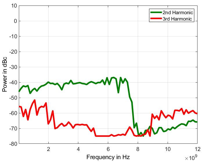
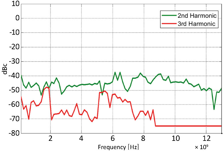
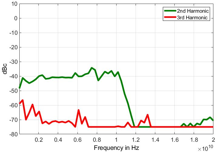
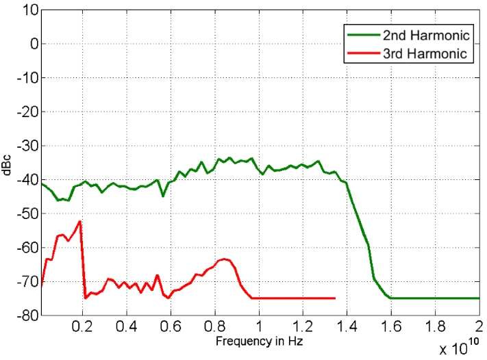
7Spectral Purity
Spectral purity at +5 dBm.
Figure 7: Harmonics, standard.Figure 8: Harmonics, 845-12 with option FILT.
Parameter
Typical
Max
Note
Output harmonics
-40 dBc
-30 dBc
See plot
845-12 with option FILT, 10 MHz to 8 GHz
-40 dBc
-30 dBc
See plot
845-12 with option FILT, 8 GHz to 12 GHz
-60 dBc
-50 dBc
845-20 with option FILT, 10 MHz to 12 GHz
-40 dBc
-30 dBc
See plot
845-20 with option FILT, 12 GHz to 20 GHz
-65 dBc
-50 dBc
845-26 with option FILT, 10 MHz to 15 GHz
-40 dBc
-30 dBc
See plot
845-26 with option FILT, 15 GHz to 20 GHz
-60 dBc
-50 dBc
Sub-harmonics
< 20 GHz
-75 dBc
-65 dBc
> 20 GHz
-50 dBc
-40 dBc
Non-harmonic spurious
CW +10 dBm, > 3 kHz offset
< 312 MHz
-80 dBc
-66 dBc
> 312 to 625 MHz
-75 dBc
-70 dBc
> 625 MHz to 1.5 GHz
-75 dBc
-65 dBc
> 1.5 GHz to 2.5 GHz
-70 dBc
-65 dBc
> 2.5 GHz to 5 GHz
-65 dBc
-60 dBc
> 5 GHz to 10 GHz
-60 dBc
-55 dBc
> 10 GHz to 20 GHz
-55 dBc
-50 dBc
> 20 GHz
-50 dBc
-45 dBc
Residual FM @ 10 GHz
15 Hz
0.3 kHz to 3 kHz, weighted (ITU-T), RMS
Residual AM @ 10 GHz
0.02%
RMS value (0.01 kHz to 15 kHz)
Figure 9: Harmonics, 845-20 with option FILT.Figure 10: Harmonics, 845-26 with option FILT.
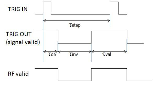
8Sweeping & Switching
Digital power / frequency / list sweeps. Sweep type: linear, logarithmic, random. Sweeps can be performed with combined internal or external AM/FM/PM/pulse modulation running; with modulation enabled, the minimum step time increases to 2 ms.
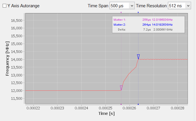
Sweep timing relationship between TRIG IN, TRIG OUT (signal valid), and RF valid, showing tstep, tde, tinv, and tval.Figure 15: Typical switching transient from 12 GHz to 14 GHz step.
Parameter
Min
Typical
Max
Note
Step time (tstep)
Standard
400 µs
19998 s
Option FS
40 µs
Dwell time (tval)
10 µs
9999 s
Off-time incl. transient time (toff)
0
9999 s
Transient time (ttnv)
Standard
270 µs
Option FS
30 µs
Timing delay (tde)
Standard
2 to 10 µs
Option FS
50 ns
Time resolution
Standard
0.1 µs
Option FS
5 ns
Timing accuracy per point
Standard
3 µs
Option FS
5 ns
9Reference Frequency
REF IN input and REF OUT output are at the rear panel.
Parameter
Min
Typical
Max
Note
Internal reference frequency
100 MHz
Initial accuracy
±40 ppb
Calibrated at 23 ±3 °C at time of calibration, user adjustable
Temperature stability (0 to 50 °C)
±100 ppb
Aging, 1st year
0.5 ppm
Aging per day (after 30 days operation)
5 ppb
Warm-up time
5 min
Output of internal reference
10 / 100 MHz
Output power
0 dBm
Output impedance
50 Ω
Bypass internal reference input
100 MHz, -5 to +10 dBm
High phase-synchronous mode
External input range (phase lock)
1 MHz
250 MHz
User programmable
Reference input level
-5 dBm
0 dBm
+13 dBm
Lock range
±1.5 ppm
Reference input impedance
50 Ω
10Outputs & Triggers
Multi-Purpose Output (FUNC OUT)
Output is FUNC OUT at the rear panel.
Multifunction generator
Min
Typical
Max
Note
Frequency range (sine, triangle, square)
Sine
10 Hz
3 MHz
Triangle
10 Hz
1 MHz
Square
50 kHz
Frequency resolution
0.1 Hz
Output voltage amplitude (peak-peak)
Sine, triangle
10 mV
2 V
Square (CMOS output)
5 V
Harmonic distortion
1%
< 100 kHz, 1 Vpp
Output impedance
50 Ω / CMOS
Sine, triangle / square wave
Video output (of internal pulse modulator)
Min
Typical
Max
Output
CMOS
Period
30 ns
50 s
Pulse width
15 ns
50 s
RF delay
10 ns
TRIG OUT synchronization modes for multiple sources: trigger on sweep start, trigger on each point, signal valid (option FS).
Trigger (TRIG IN)
Input is TRIG IN at the rear panel. Trigger Output (TRIG OUT) follows the Multi-Purpose Output (FUNC OUT) above. See the sweep timing diagram in the Sweeping & Switching section.
Parameter
Min
Typical
Max
Note
Trigger types
Continuous, single, gated, gated direction
Trigger source
RF key, external, bus (GPIB, LAN, USB)
Trigger modes
Continuous free run, trigger and run, reset and run
Trigger latency
Standard
2 µs
Option FS
130 ns
Trigger uncertainty
Standard
5 µs
Option FS
10 ns
External trigger delay
Standard (programmable)
50 µs
40 s
Option FS
50 ns
10 s
External delay resolution
Standard
15 ns
Option FS
10 ns
Trigger modulo
1
255
Execute only on Nth trigger event
Trigger polarity
Rising, falling
External trigger input threshold
0.85 V
0.9 V
0.95 V
TTL compatible
External trigger input voltage range
-0.5 V
+5.5 V
TTL compatible
External trigger input hysteresis
60 mV
11Modulation
Combinations of AM/PM/FM/pulse are possible. See the user manual for more details.
Pulse Modulation
Parameter
Min
Typical
Max
Note
On/off ratio
75 dB (typical)
At +10 dBm
Repetition frequency
DC
10 MHz
Pulse width
ALC hold
100 ns
5 s
ALC hold, options NP or FS
30 ns
5 s
ALC on
500 ns
Pulse rise/fall time
< 5 GHz
30 ns
> 5 GHz
5 ns
Duty cycle
0.05%
99.95%
Pulse resolution
30 ns
Polarity
Selectable
External input threshold
0.85 V
0.9 V
0.95 V
TTL compatible
External input voltage range
-0.5 V
+5.5 V
TTL compatible
External input hysteresis
60 mV
Delay (to RF)
20 ns
40 ns
Pulse Pattern Modulation
Using internal pattern generator.
Parameter
Min
Typical
Max
Note
Pulse bit width
ALC hold
100 ns
ALC hold, or FS ALC on
30 ns
ALC on
500 ns
Programmable pattern length
2
4096
Duty cycle
0.05%
99.95%
Pulse bit resolution
Standard
30 ns
Option FS
5 ns
Polarity
Selectable
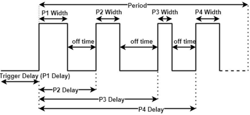
N-Pulse Modulation (Option FS)
N-pulse modulation timing parameters: P1 to P4 widths, delays, off times, and period.
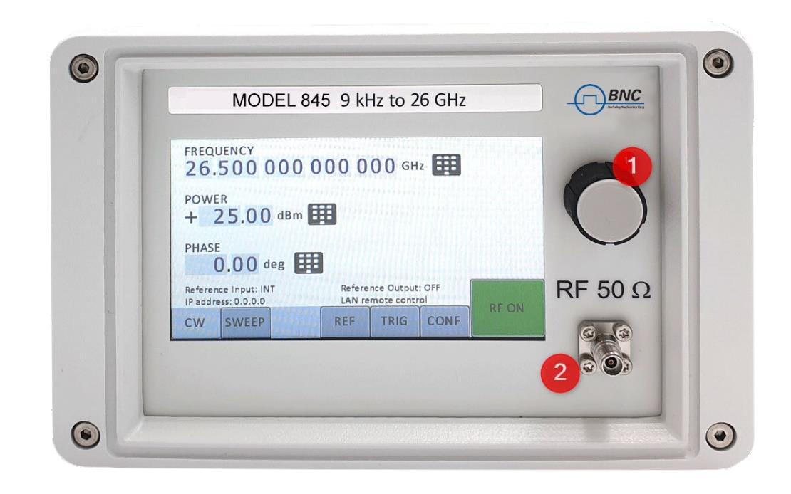
Front panel (touch screen version): rotary knob/button (1) and RF 50 Ω connector (2).
Rotary knob / button: The rotary button is used to change the value selected on the screen.
RF 50 Ω connector: This female N-type or SMA connector provides the output for generator signals. The impedance is 50 Ω. The reverse power damage level is +30 dBm maximum. The maximum allowed DC level is ±10 V. Please check the data sheets for more details.
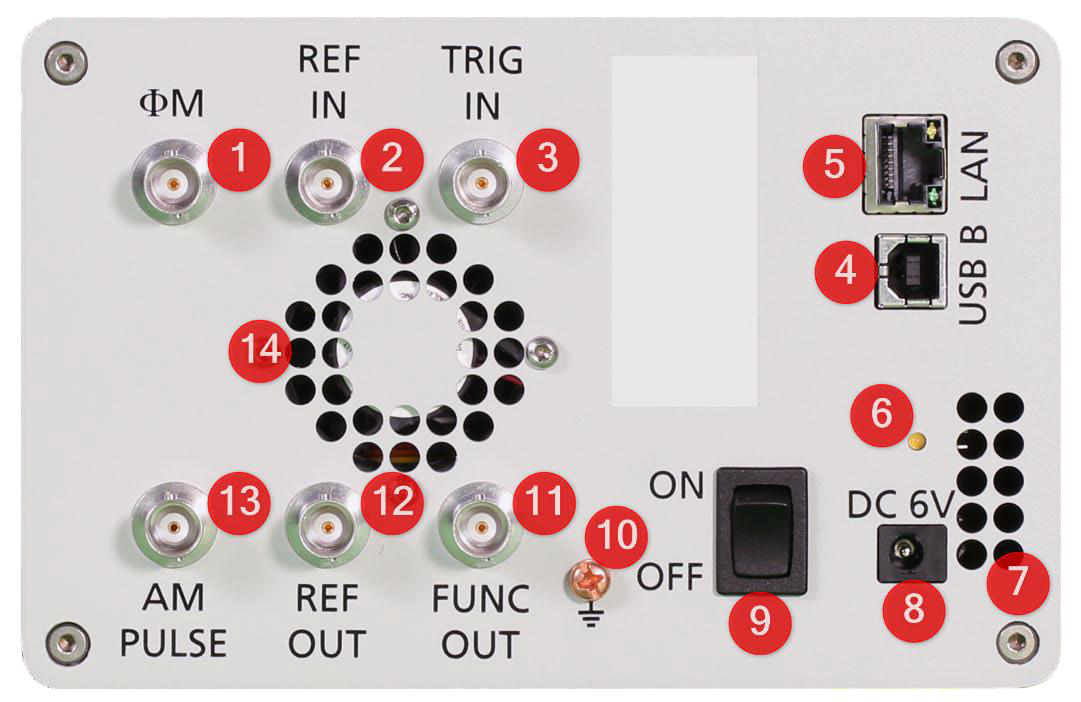
Rear Panel
Rear panel connectors and controls (numbered 1 to 14).
ΦM: This BNC female connector is the input for FM and PM.
REF IN: This BNC female connector is the input for the reference signal.
TRIG IN: This BNC female connector is the trigger input.
USB B: The USB B connector is used to connect the device to a computer.
LAN: The LAN connector is used to connect the device to a network.
Battery LED: In case the device has a rechargeable battery, this LED indicates whether the battery is charged or not.
Fan holes: The air intake of the fan.
Power supply: Connect the BNC power adaptor to this connector to supply the device with energy.
ON/OFF switch: Turns the device on or off.
Ground screw.
FUNC OUT: This BNC female connector is the output for the function signal.
REF OUT: This BNC female connector is the output for the reference signal.
AM PULSE: This BNC female connector is the input for the AM and the PULSE modulation signal.
Fan holes: The holes by which the air is extruded.
13Ordering Information
Host model
Product / option
Description
845-12
845-12
12 GHz microwave signal generator
845-20
845-20
20 GHz microwave signal generator
845-26
845-26
26 GHz microwave signal generator
845-12/20
Option 9K
Frequency range extension to 9 kHz
845-26
Option PE
Mechanical step attenuator (26 GHz version) down to -90 dBm
845-XX
Option PE2
Mechanical step attenuator to -120 dBm
845-XX
Option HP
Higher output power
845-12/20/26
Option FILT
Improved harmonic filtering
845-XX
Option FS
Ultra-fast switching speed (export control)
845-XX
Option FLASH
MicroSD card slot for removable SD memory
845-XX
Option IEC
IEC 17025 calibration with certificate
845-XX
Option Bag
Portable bag
845-XX
Option GP08 / GPIB
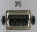
GPIB interface.
GPIB interface connector.
845-XX
Option EB6
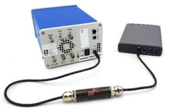
External power bank adapter cable with voltage converter for 12 to 25 V supply. Required input connector: inner / outer diameter 2.1 / 5.5 mm.
Model 845 powered from an external battery pack via the Option EB6 adapter cable.
845-XX
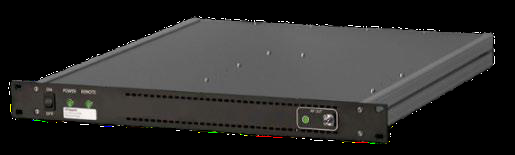
Option 1URM
19" 1U rack-mount module. Dimensions 1.7 in H x 16.8 in W x 18.1 in L [42 mm H x 426 mm W x 460 mm L].
19" 1U rack-mount module (Option 1URM).
845-XX
Option RM
19" 3U rack-mount kit
845-XX
Option REAR
Move output to rear panel
845-20/26
Option OEM
OEM package
845-XX
Option Retrofit
Applies when options are added after first delivery
The options PE3 / GPIB cannot coexist in the standard desktop housing. Please choose a maximum of two of them. No restriction with option 1URM.
When PE or PE2 is chosen, GPIB can no longer be selected.
The options REAR and GPIB cannot be ordered together.
For a configured quote, contact Berkeley Nucleonics Corporation · info@berkeleynucleonics.com · 415-453-9955.
14General Characteristics
EMC complies with the EMC regulations and directives for emission and immunity to interference (EN 61326-1 Industrial, EN/IEC 61326-2-1). Safety complies with the applicable safety regulation in line with IEC/EN 61010-1.
Characteristic
Specification
Remote programming interfaces
Ethernet 100BaseT LAN interface; USB 2.0 host & device; GPIB (IEEE-488.2, 1987) with listen and talk (optional)
Control language
SCPI version 1999.0
Power requirements
6.25 ±0.2 VDC; 20 W maximum
Main adapter supplied
100–240 VAC in / 6 V, 6.0 A DC out
Environmental
Levels similar to MIL-PRF-28800F Class 3 & 4. Samples type tested to be robust against the environmental stresses of storage, transportation, and end-use (temperature, humidity, shock, vibration, altitude, and power line conditions).
Operating temperature range
0 to 45 °C
Storage temperature range
-40 to 70 °C
Max. relative humidity
85% up to 45 °C ambient
Operating and storage altitude
Up to 15,000 feet (4600 m)
EMC
Complies with EMC regulations and directives for emission and immunity to interference (EN 61326-1 Industrial, EN/IEC 61326-2-1)
Safety
Complies with applicable safety regulation in line with IEC/EN 61010-1
Weight
≤ 6 lbs (2.5 kg) net, ≤ 8 lb (4 kg) shipping
Dimensions (H x W x L)
4.60 in H x 6.83 in W x 10.30 in L incl. connectors [116.9 mm H x 173.6 mm W x 261.7 mm L]

 EMC complies with the EMC regulations and directives for emission and immunity to interference (EN 61326-1 Industrial, EN/IEC 61326-2-1). Safety complies with the applicable safety regulation in line with IEC/EN 61010-1.